1. I don't get it. One MTH photo shows 4 flying-lead bare-wires and the other shows the 4 wires in a connector plug?
2. What's the space on that MTH connector - looks like 2.54mm (0.1")? That looks like a standard connector family but that's easy for me to say! As you know you go to digikey and try to punch in a few parameters and still come up with a zillion choices. Maybe someone in the know will identify the manufacturer and series designation. But in general, as long as you get the pitch correct and leave enough clearance, if/when you find the right connector it should drop into the PCB.
If re-doing the PCB, I suppose you should change the order of the 4-terminals from G-Y-R-com (as is) to R-Y-G-com (MTH style).
You might also look to see if a standard square-pin male connector (non-polarized) securely mates with the MTH plug. That is, this saves the trouble of tracking down the connector family. So you lose the benefit of polarity and would have to be mindful to plug in the MTH connector plug in the correct orientation.
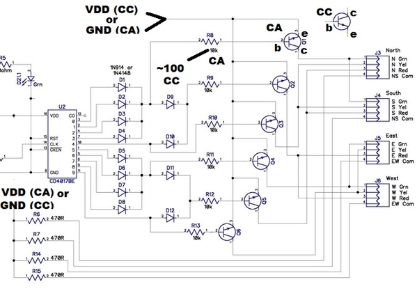
3. The Common Anode (CA) vs. Common Cathode (CC) is interesting. First off, the original design was a common cathode configuration. That is, you could simply take the 6 signals (RYG E-W, and RYG N-S) BEFORE the 10K resistor and Base input to the transistors and attempt to drive the MTH CC signal head(s). In other words you could do this today with the hardware you have.
4. But, if this is too dim or you want a dual-purpose (CC or CA) alternative with what I understand is your latest version of the PCB:
a) install the 6 transistors "backwards". That is, rather than CBE for pins 1-2-3, rotate the NPN transistor 180 degrees. The B is still the middle pin but you are swapping the E and B terminals of the transistor. This makes the NPN transistor into a non-inverting buffer using the so-called "emitter follower" configuration. So you get the benefit of additional current driving capability (i.e., the buffering) that a transistor brings to the table.
b) as shown, the 6 transistor emitter at the top which previously went to GND for CA now go to VDD.
c) as shown, the 4 resistors at bottom which previously went to VDD for CA now go to GND.
Note that unless your PCB layout software did something weird, you should be able to cut a single trace for b) and c) and on the bench simply tack the wires to the opposite power supply rail (VDD become GND, GND becomes VDD). Or if re-designing a PCB, you'd make, say, a 3-terminal 0.1" header with the VDD on pin 1 and GND on pin 3. Then use a push-on programming jumper to steer pin 2 to either 1 or 3 depending on the CA vs. CC application.
d) lower the value of the 6 resistors from 10K for CA to, say, 100 ohms for CC.
e) there is a somewhat analogous method to use N-channel FETs to implement what's know as a source-follower non-inverting buffer (vs. the NPN transistor emitter-follower non-inverting buffer) but it gets tricky so I don't want to go there.
5. The on-off switch function should not require a PCB modification - just cut power to the board with a toggle switch.
6. If the lower voltage works I see no problem operating the circuit at 5V or 6V. You will need to lower the values of the 4 resistors in the common leg of the LEDs.
I think I addressed the issues at hand. Whew! ![]()


