Hi Again...
Okay so I had like >25 people ask me about how to decode the DCS packets today from the other post about how to view the signals with a scope. The simple answer is: it's not too simple but I'm both a integrated circuit designer, and an educator, so I will take on the challenge of explaining it for everyone.
==============
Quick Refresher
==============
So from the other post [Viewing DCS DS/SS] we talked about how DCS uses direct sequence spreading and how each bit is actually represented by 31 spreading-chips that make up a PN code.
Again imagine I have a packet I want to send from the TIU to the train, and for each bit (1 or 0) in that packet, I replace that bit with a PN code:
If I see "1" I put some 31 chip code into the track "00110101110111001101010111001100101"
If I see "0" I put the opposite 31 chip code into the track "11001010001000110010101000110011010"
Okay great so how do we get our original code back?
==============
De-Spreading
==============
The process of turning the 31 spread-chip PN-codes back into each the single 0 or 1 in our packet is called de-spreading. Essentially we need to build a circuit that looks at the code on the track and compares it to the known code and identifies it as either the one or zero code.
Even though the real DCS system is 31 bits, I don't want to type all night so lets pretend its only 5 bits long.
Imagine we have a DCS-like 5-chip ds/ss system where
PN for 0 = "11011"
PN for 1 = "00100"
and we want to send the packet 101.
The transmitted sequence will be 00100 11011 00100
Clock Considerations:
Okay cool. So the first thing we need to think about is the clocking scheme. The chips in the transmitted sequence are updated at a rate of 3.75MHz meaning that every 266ns we will see the next symbol on the track. Now if we also clock the receiver at the same speed, in theory we will get 1 copy of each sample into our locomotive and can start comparing to the known PN codes. The trick is that in reality this does not work becasue your receiver will sample at Ttrain= n(266ns) + To1 (where to is the initial delay) while the TIU transmitter is putting the data onto the track at Ttiu= n(266ns) + To2. If you're really unlucky with To1 and To2 (which are simply a function of when you turn the TIU and train on) you could have the situation where the train receiver is looking at the track in the same instant the TIU is transitioning between values. Since the value is changing while you are trying to read it under this condition, you end up with a mess and nothing is reliably received. In comm system design we call this problem " clock synchronization", and the general set of solutions are called Clock-Data Recovery or "CDR" for short.
Basically there are 2 categories of techniques for CDR to align the transmitter and receiver clocks.One is called "phase-tracking" and the other is called "Phase-picking".
->Phase tracking solutions use a phase-lock loop to generate the receiver clock at the same frequency as the transmitter by directly locking on the transitions between chips. They then delay the locked clock by exactly T/2 (133ns in this case) to make sure the receiver is always sampling at the instant in the middle the last and next transition of the transmitter:
TX Clock edges: X X X X X (time where data changes)
RX Clock edges: X X X X (time where data is read)
It's not used in DCS but it's the 99.999% more common way to solve clock synchronization, if you open a modern Qualcomm baseband modem, this is what's in there.
-> Okay so phase-picking (the one that DCS uses). What we do in phase-picking is say we know the data is changing every 266ns, so if I take samples at 133ns (twice as fast), I know that at least one of every two samples will be at a time when the data is not changing.
TX Clock edges: X X X X (time where data changes)
RX Clock edges: X X X X X X X X (time where data is read)
So what we do is sample at twice the rate (3.75MHz X 2 = 7.5 MHz) and then we are covered... sort of. Time for more of the hardcore details.... In general you can imagine with this approach that if a given sample n is bad, then the next sample n+1 is probably okay, and the sample after that is probably bad again. Basically we assume that either (all the even samples we took) , or (all the odd samples we took) will be good. So we actually build two receivers in parallel, one looking at the even values and one looking at the odd values.
Okay so this assumption has 1 big conditional. It's only true if one clock frequency is exactly twice the other. This is of course not true in practice as the clocks will drift a little. So right now we have spreading-chips coming every 266ns and we're sampling at 133ns. Lets say for example the Rx clock was a bit off so we had 266ns and 132ns. This means in the RX two samples will be 132X2 = 264ns, meaning we will start sampling (266-264)=2ns early on the next spreading-chip. 2ns compared to 266ns so that is not a big deal. So the next chip was expected to start at 266ns but really starts at 264ns and then it's only 264ns long too, so when we expected to end 2 chips at 266X2=532ns we actually ended at only 528ns (4ns error). The longer we make the packet the more the chip-to-chip slip (called cycle slippage in communication design). Typically we design what we call the "coherence span", which is the total number of chips you can have over which the slip is less than half of the chip time at the end of the entire sequence. In this case the chip time is 266ns (and a half-chip time is 133ns), and we're slipping 2ns each chip so 133/2= 66 chips is the most we can send for each packet. In reality 1ns/133ns is a really big error, typically in ds/ss systems we talk about clock frequency errors in the parts per million. Still, the "coherence-span" is the fundamental parameter in a communication system that limits how long a packet can be.
For those interested: Phase tracking also has a coherence-span, which is related to how well the phase-lock loop can hold phase over time (called phase noise or timing jitter).
Okay cool, so that's the clocking out of the way. On to the decoding
Decoding part:
Okay so now we sampled the incoming packet correctly. Remember from here on we actually do everything on two copies (then even samples and the odd samples), but I will leave that out of this part to make it easier to understand.
So thinking about our DCS-like code coming in to the receiver that we sent in the above example:
00100 11011 00100
It will actually be time dependent at the receiver, that is we will receive one byte at a time. We can use a thing called a shift register that stores bits in the sequence they were received in:
[D4]->[D3]->[D2]->[D1]->[D0]
This is a 5 bit shift register.... when the first clock comes the track data moves into D5, whatever was in D5 before moves to D4, what was in D4 moves into D3 and so on down to D0. The data that was in D0 is just forgotten.
So imagine we are receiving a sequence like 01001 as an example. In time what will happen is
start: D4=X D3=X D2=X D1=X D0=X
after 1 clock: D4=1 D3=X D2=X D1=X D0=X
after 2 clock: D4=0 D3=1 D2=X D1=X D0=X
after 3 clock: D4=0 D3=0 D2=1 D1=X D0=X
after 4 clock: D4=1 D3=0 D2=0 D1=X D0=X
after 5 clock: D4=0 D3=1 D2=0 D1=0 D0=1
(x are values we don't know.... becasue we don't know what was inside to begin with)
So what we do next is cool. We use XNOR gates.
An XNOR gate is a circuit with 2 inputs and 1 output. If the 2 inputs are the same (both 0 or both 1) it outputs a 1, if they are different it outputs a zero.
1 XOR 1 = 1 0 XOR 1 = 0 0 XOR 1 = 0 0 XOR 0 = 1
Okay cool.
So we can put the XOR between the known PN_code and the shift register. When they match we can write down that we received a 1 or 0 accordingly. Mathwise:
Our PN_code is {PN4 PN3 PN2 PN1 PN0}
When we have (PN4 XOR D4)=1 AND (PN3 XOR D3)=1 AND (PN2 XOR D2)=1 AND (PN1 XOR D1)=1 AND (PN0 XOR D0)=1 it means we have a match. The next step is we add up all the xor results.
So lets say our PN code was the 11011 from above and we had a 01010 in the shift register at this instant. Then the XOR output would be
11011
01010
=====
01110 (0 when they don't match, 1 when they do)
We can add these up to get 0+1+1+1+0 = 3
We call this summation the "code-correlation".
So the more numbers that match, the closer the input code is to the known PN_code in our memory and the higher our code correlation. Now remember that our PN_code for 0 is the opposite of the PN_code for 1.
So if the result is totally different than our PN_code for 1, the code-correlation will be 0 (which means the shift register data exactly matches our code for 0).
What's the Probability of false detection of our PN code:
This is where it gets interesting if you want to do some statistical analysis....
The real DCS code is 31 chips.
Now imagine we pick 31 random values of 1 and 0 and assemble them into a chip code. Basically this is the same as guessing 1 or 0 thirty-one times. You would expect about 50% of the bits you you guessed to be right which means of the 31 chips, about 15 would be correct. Going through the shift register and XOR, this means that the code-correlation will have a statistical mean somewhere around 31/2 (so about 15.5).
Short hand note: often we call code-correlation "Cx" for short. So some statistics now
we would say the expected value of Cx or E(Cx) = 15.5
So choosing 1 or 0 has equal probability (called a binomial probability distribution). The statistical variance Var(Cx) is going to be (1-0.5)/0.25 or about 2, or a standard deviation of about sqrt(2). This means that if we randomly pump data in 99% of the time the Cx will land within 3 standard deviations of the mean (IE between 15.5 - 3Xsqrt(2) and 15.5+3Xsqrt(2)) or (11.3 to 19.7). So if we consider 6 standard deviations next ( 6sqrt(2) = 8.4) that means that a random stream of data has a 1 in 506,797,356 chance of providing a Cx outside the range of 7.1 to 23.9. What this is really saying is there is less than a 1 in 500 million chance of accidently matching (31-7) = 24 bits or more.
Similarly for completeness:
Matching 25 bits or more is about a 1 in 13 billion chance
Matching 27 bits or more is about a 1 in 16.2 trillion chance
Okay so the chip time was 266ns right? (266x 10^-9 s) so receiving 16.2 trillion chips would take 4 million seconds (about 50 days). So unless you run the train for 50 days straight you will never see enough chips to have 27 spreading-chips matched randomly....
Confidence Threshold:
Right okay so all the statistics was to set up this concept. Remember we said that when:
Cx=0 means all the bits are matching the PN_code for 0
Cx=31 means all the bits are matching the PN_code for 1.
Well sometimes the track contacts can glitch or we go over a turnout switch and lose a bit or something... so is it really necessary to only detect when all of the code matches? Remember that one in 16.2 trillion chance above.
So we define a confidence threshold value called "Ct"... basically a number that says "if more than this many bits match" we still take it as a 1 or 0 in our packet.
Right so back to the 5 chip example:
Lets set the confidence threshold to 4
so if we have a PN_code of 11011
and we receive
11011 (the right code)
then the Cx=5 and (Cx=>Ct) so we take the number.
Similarly
if there's a glitch and receive
11(1)11 (one flipped chip)
then the Cx=4 and still (Cx=>Ct) so we take the number.
This is the big advantage of ds/ss is that it's error tolerant. So then we get into fundamental optimization concepts. In the DCS system Ct has values from 15 to 31. (Its not 0 to 31 because Cx going from 0 to 15 means we're matching the 0 code instead of the 1 code). If we make Ct very high ... say 30 or 31, then the probability of random error is very low, like 1 in quadrillions, but the tolerance to flipped bits is low (none or only 1 bit can be flipped) , alternatively if we lower Ct to like 25, then we can tolerate a lot of errors, but the probability of a false detection is also going up a lot... So you have to design a Ct that's reasonable at both ends of the scale. The "signal strength" you see on the remote is actually the Cx values added up for all the bits in the packet with some scaling applied.
So usually once you've detected those 1's and 0s for the packet, you put them into an packet-buffer with an index register that counts how many bits you've received so far. A separate circuit (not discussed here... maybe later) called a command decoder recognizes those packet sequences as commands. Each time a command is detected, the command decoder resets the index counter to 0 and clears the packet buffer so that the ds/ss receiver becomes ready to receive the next packet sequence. Unfortunately all of these are inside the programmable on the PS2/3 boards so they aren't accessable (unless you build your own chip ![]()
------------------------
Example Stuff
------------------------
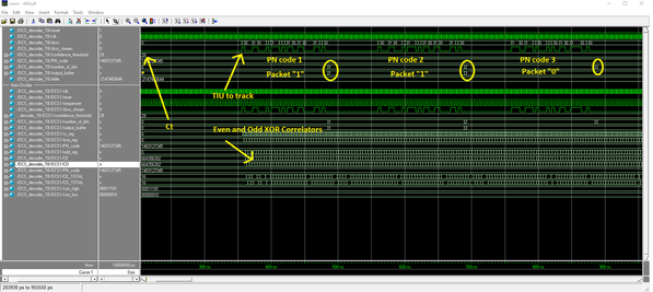
Right so that's everything you need to know to design a circuit to decode a DCS packet. Just build exactly that. I just built one for FPGA / ASIC platforms in parallel while I was writing this post to make sure no steps were missed. Here is the modelsim output:
Below is the RTL code (verilog 2001 format) used to build this DCS hardware. I will just paste it into the post and hope the forum has mercy on the format. I haven't had a chance to try it on FPGA yet but I will in the coming weeks. For those not familiar with building digital systems (processors or decoders and such) RTL is not a programming language, but instead is used to describe hardware. It can be synthesized (not compiled) into either an FPGA (programmable chip) or a hard ASIC (dedicated silicon like I build at JPL). For those new to RTL, it's not like C++ thinking... every single line in the code executes at the same time (when the clock edge shows up!)
Note: In this RTL the known PN_code comes from outside.... so you can set it to whatever you want. Again I don't want to give anyone the MTH PN_code in post, so consider it your homework to figure out what value needs to go there. Between this and the other post, it should be super obvious.
------------------------------------------------------------------------
Adrian's Example RTL (digital implementation) for a DCS decoder
----------------------------------------------------------------------
//
//
// DCS Decoder Block Version 1.00 for FPGA/ASIC targets
// Adrian Tang 2016
//
// You need to clock at twice the spreading-chip rate (IE 7.5 MS/s)
// Verilog 2001
//
// Typically a good PN code will be same number of 1s and 0s for minimal DC
//
// Usage
//
// 1. Reset the block.
// 2. As PN_codes are recognized the bits they represent will be added to the output buffer
// 3. number_of_bits holds the current index of the output buffer
// bits from output_buffer[0] to output_buffer[number_of_bits-1] are valid
// 4. The actual command decoder block (not implemented) should look at output buffer and when it recognizes the packet
// reset this block to prepare for capturing the next DCS packet
//
module DCS_decoder(reset, clk, dsss_stream, confidence_threshold, PN_code, number_of_bits, output_buffer);
//Main Decoder Block Control
input clk; //mater clock on the block (7.5 MS/s)
input reset; //master reset for the block tripped after each packet
reg sequencer;
//Block Inputs
input dsss_stream; //dsss stream from track
input [30:0] PN_code; //Fixed PN Code input
input [7:0] confidence_threshold; //Confidence Threshold Level
//Block Outputs
output [7:0] number_of_bits; //Counts the number of bits detected
reg [7:0] number_of_bits;
output [255:0] output_buffer; //Actual output data
reg [255:0] output_buffer;
//Internal registers
reg [61:0] sr_reg; //Input shift register packet streams into
reg [30:0] eve_reg; //Even phase subregister for decoder
reg [30:0] odd_reg; //Odd phase subregister for decoder
//intermediate correlation values
reg [30:0] CE; //even phase correlation
reg [30:0] CO; //odd phase correlation
reg [7:0] CE_TOTAL; //Accumulated even confidence
reg [7:0] CO_TOTAL; //Accumulated even confidence
//Confidence Intervals for dsss
wire [7:0] con_high;
wire [7:0] con_low;
//---------------Generate the tow level confidence levels------------------------------
assign con_high = confidence_threshold; //we need more than (confidence_threshold) out of 31 spread chips to match to take it as 1
assign con_low = 7'd31 - confidence_threshold; //we need more than (confidence_threshold) out of 31 spread chips NOT to match to take it as 0
//----decoder core operation begins here
always@ (posedge clk)
begin //always on clock synchronous operation
//------------------------------------------------------------------------------------------------------------------------------------------------------------------------
// MAIN CORRELATION
//------------------------------------------------------------------------------------------------------------------------------------------------------------------------
//input 62 bit shift register to take in the track data
sr_reg <= sr_reg >> 1;
sr_reg[61] <= dsss_stream;
//-----------------Assign the odd and even registers from the main shift register in order to cover both possible phases----------------
odd_reg <= {sr_reg[60],sr_reg[58],sr_reg[56],sr_reg[54],sr_reg[52],sr_reg[50],
sr_reg[48],sr_reg[46],sr_reg[44],sr_reg[42],sr_reg[40],sr_reg[38],
sr_reg[36],sr_reg[34],sr_reg[32],sr_reg[30],sr_reg[28],sr_reg[26],
sr_reg[24],sr_reg[22],sr_reg[20],sr_reg[18],sr_reg[16],sr_reg[14],
sr_reg[12],sr_reg[10],sr_reg[8], sr_reg[6], sr_reg[4], sr_reg[2],
sr_reg[0]};
eve_reg <= {sr_reg[61],sr_reg[59],sr_reg[57],sr_reg[55],sr_reg[53],sr_reg[51],
sr_reg[49],sr_reg[47],sr_reg[45],sr_reg[43],sr_reg[41],sr_reg[39],
sr_reg[37],sr_reg[35],sr_reg[33],sr_reg[31],sr_reg[29],sr_reg[27],
sr_reg[25],sr_reg[23],sr_reg[21],sr_reg[19],sr_reg[17],sr_reg[15],
sr_reg[13],sr_reg[11],sr_reg[9], sr_reg[7], sr_reg[5], sr_reg[3],
sr_reg[1]};
//-------------Generate the 4 correlation terms--------------
//Even Phase Positive
CE <= eve_reg ~^ PN_code;
//Odd Phase Positive
CO <= odd_reg ~^ PN_code;
//-------------Compute the total correlation--------------
CE_TOTAL = CE[30] + CE[29] + CE[28] + CE[27] + CE[26] + CE[25] + CE[24] + CE[23] + CE[22] + CE[21] +
CE[20] + CE[19] + CE[18] + CE[17] + CE[16] + CE[15] + CE[14] + CE[13] + CE[12] + CE[11] +
CE[10] + CE[9] + CE[8] + CE[7] + CE[6] + CE[5] + CE[4] + CE[3] + CE[2] + CE[1] +
CE[0];
CO_TOTAL = CO[30] + CO[29] + CO[28] + CO[27] + CO[26] + CO[25] + CO[24] + CO[23] + CO[22] + CO[21] +
CO[20] + CO[19] + CO[18] + CO[17] + CO[16] + CO[15] + CO[14] + CO[13] + CO[12] + CO[11] +
CO[10] + CO[9] + CO[8] + CO[7] + CO[6] + CO[5] + CO[4] + CO[3] + CO[2] + CO[1] +
CO[0];
if(reset==1)
//if the block is in reset mode
begin
number_of_bits<=8'd0; //reset the bit counter
output_buffer<=256'd0; //Clear the output buffer
sequencer<=1'b0;
end
else
//if the block is running
begin
sequencer <= ~sequencer; //This ones a bit complicated. Ideally we have two samples per spreading chip but we don't want to double count
if(sequencer==1) //as the chip moves from the even side to the odd side, so we only look at both even and odd every 2 clocks
//to prevent double counting the same PN_code
begin
//-------------Decode to the output packet buffer--------------
//If we have a "1" PN_code detected
if ((CE_TOTAL > con_high) || (CO_TOTAL > con_high))
begin
number_of_bits <= number_of_bits + 8'd1; //increment the bit counter
output_buffer[number_of_bits] = 1'b1; //Set the output buffer to a 1 if we detected a 1
end
//If we have a "0" PN_code detected
if ((CE_TOTAL < con_low) || (CO_TOTAL < con_low))
begin
number_of_bits <= number_of_bits + 8'd1; //increment the bit counter
output_buffer[number_of_bits] = 1'b0; //Set the output buffer to a 1 if we detected a 1
end
end //sequencer
end //reset =0 condition
end //on clock edge
endmodule
------------------------------------------------------------------------
Conclusions:
----------------------------------------------------------------------
So now everyone knows exactly what's going on inside. I'm not trying to go hardcore circuit and system design, but honestly that's what you need to know if you really want hardware that decodes those DCS packets.
Anyways hope this is educational to everyone and useful to someone
Adrian J Tang
slowly converting model railroading into science


